Nicholas G. Usechak
AFRL – Sensors Directorate, Wright–Patterson, OH 45433
1. Introduction
The field of advanced photonics research and development has rapidly evolved over the past few decades. Today, working in photonics presents unique challenges, especially for those performing research and development involving hardware. These difficulties exist not only for small photonics companies, but across all sectors including large companies, academia, and government laboratories.
Long gone are the days when large vertically integrated companies (such as Bell Labs) were the norm — today research is conducted differently than in years past. This month’s column comments on the trends that have occurred over the past few decades and discusses what appears to be inspiring funding organizations now and will perhaps continue to do so for the next 5 to 10 years.
2. The Changing Landscape
Looking back on the last 50 years of photonics research and development, there have been a number of large shifts. A good portion of the research conducted in the 1970s and 1980s involved free-space optics and lens-based systems. Starting in the late 1980s, and continuing over the next few decades, this evolved into a focus on optical fibers and fiber-based/fiber-connected devices.
In the 1980s through the 2000s, the use of fiber-pigtailed “commercial off-the-shelf” technologies enabled researchers to explore and create (what at that time were) complex systems in their own labs with little more than a fiber fusion splicer. While work using these devices is still important and continues to this day, such systems frequently suffer due to environmental effects, tend to be time-consuming (i.e, expensive) to build, and are hard to scale. Consequently, many today have grown to view them as “legacy”. This has led to the desire to find new solutions or “what’s next” — not only among researchers but also within funding organizations. Sometimes what’s next is not a single technology, and sometimes it is the last technology that was going to be “the next big thing” last time. This happens when research takes too long to develop (or at least too long for the attention span of funding organizations) or fails to yield results that live up to its hype. In these cases, funding organizations frequently lose interest and walk away from such investments. Sometimes people re-discover some of these fields decades later. Examples of areas that did not change the world as initially envisioned when first explored include resonator-based biosensing (~2000) and metamaterials (~2010). Other areas that have perpetually been the next big thing include fields of research such as quantum computing and optical computing (both of which are experiencing strong interest today).
While the technical forefront of optics and photonics continues to evolve, it has also slowly given way to new challenges and opportunities that often require resources beyond what are accessible internally for many organizations. Frequently, it is these changes that make something that was not previously viable, warrant renewed interest.
I think it is also helpful to consider the large scale changes that have happened across industry over the last century. Although it does not provide clarity on where all sectors will end up, it does at least allow one to understand the trajectory some areas are on.
2.1. Vertically Integrated Companies
While many, if not most, researchers in photonics have a particular affection for Bell Labs [1], the onset of modern vertically integrated companies that perform research and development in the physical sciences really took off a little earlier. Indeed, between the mid-1850s and the early 1900s, pioneers such as Thomas Edison and George Eastman were hard at work and many well-known companies were founded during this time including Corning, 3M, Dupont, General Electric, IBM, etc.

These companies were not always large, and many (if not all) are far smaller today than they once were. Nevertheless, there was a time when they all had the resources to dominate their respective sectors and source not only much of their own technology but also to perform their own research. In fact, the type of research that was done by these organizations has been characterized as “custom,” to differentiate it from research performed on the side of (or outside of) one’s normal job “small,” or that tied directly to a business unit and known as “repeatable” — following the definitions found in Ref. [2].
Things started to change in the 1980s and, while it took some time, these companies no longer exist today as they once did: Bell Labs does not dominate the fields of networking and communications, IBM no longer runs its own semiconductor foundry, GE has spun off many of its subsidiaries, Kodak is a shadow of its former self, etc.
Things have changed so much (at least in the US) that today the dominant employers in many regions of the country are large universities and hospital systems, not hardware companies. Modern technology companies that have (until recently at least) appeared to remain immune to contraction include Microsoft, Google/Alphabet, Amazon, Meta, and others. These companies all have one thing in common: they have largely focused on software and not hardware. This has left a void regarding how to best accomplish hardware development, research, innovation, and production.
2.2. The Growth of Academic Solutions
In the photonics community, the bursting of the telecom bubble, which followed right after the dot-com bubble burst in the early 2000s, was catastrophic for many in the industry [3]. As a consequence of this disruptive change, much of the exploratory research being conducted in industry was either jettisoned or re-focused on near-term needs in support of existing (or upcoming) products with a focus on revenue. This change also resulted in an overall contraction of the commercial sector and motivated many highly skilled researchers to leave industry and seek academic jobs.
For the field of photonics, this resulted in a disruptive change — however, industry’s loss was academia’s gain. Previously, there were only a few US graduate schools offering an education in photonics (most notably the University of Arizona, the University of Central Florida, and the University of Rochester) and a few other well-known researchers scattered about the academic landscape — typically residing in electrical engineering or physics departments at a few dozen schools (with some clusters here and there). Today, many universities have multiple professors with backgrounds in photonics who perform active research in the field.
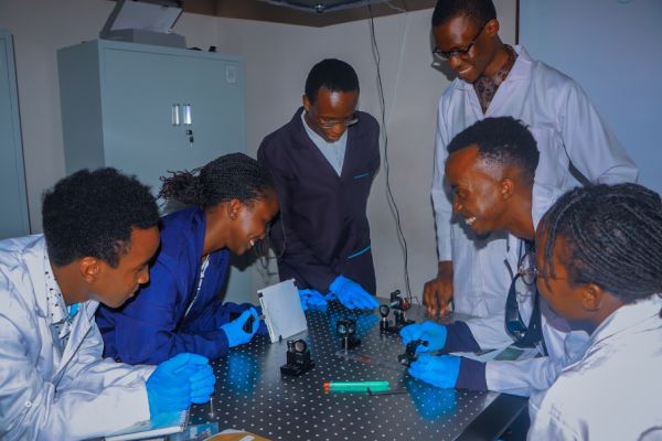
This change also resulted in professors with industrial backgrounds (from companies that were once vertically integrated) showing up in academic institutions. As funding opportunities emerged in areas like “nanotechnology,” university cleanrooms became more capable to the point where companies sought access to them to support their commercial fabrication needs. There are now a significant number of small companies that have grown over time to offer capabilities by leveraging funding from Small Business Innovation Research (SBIR) and Small Business Technology Transfer (STTR) programs (see Ref. [4]) while performing fabrication using the resources amassed in cleanroom facilities at schools such as the University of California, Santa Barbara.
Such cleanrooms have, in general, not been created to solely support photonics research but rather support microelectronics research in general. Nevertheless, researchers working in areas such as micro-electromechanical systems (MEMS) and integrated photonics have been able to piggyback on these investments and augment the tools with some specialty capabilities in these facilities to support work in their respective fields. This has enabled vibrant research to continue in the US unabated, despite the significant change that occurred in industry. However, this has also meant that the companies of today look vastly different than the companies of the past. For anyone seeking to create a startup photonics company today, it may mean you will end up employing 30 – 100 people if you are very successful — odds are you will never grow to have 20,000 or more employees. To put this in perspective, Kodak employed almost 80,000 as recently as 2000 [5]. Meanwhile, ThorLabs only lists itself as having > 1,500 employees [6], which is probably similar to the number of professors at a good size state university.
For many companies, partnering with academic institutions is a good solution and, in certain fields (e.g., where access to advanced cleanroom facilities, fiber draw towers, or other expensive infrastructure is required) it is necessary due to the upfront investment needed to build such a business from scratch [See Note 1]. Despite the advantages associated with working with/in academic institutions, there are also drawbacks. Frequently the tools needed to support corporate work are the same tools used for academic research and employees must become adept at re-qualifying them every time they are used due to process drifts. This not only becomes arduous but is highly problematic for those seeking to develop a commercial business. While relying on “drifting” tools may be bemoaned by university researchers, it makes it impossible for companies to maximize yield or guarantee performance.
2.3. Today’s Public-Private Partnership “Experiment”
As a result of these complications and with a desire to do something different and re-focus on US manufacturing, the Office of the Undersecretary of Defense (OUSD) and members of the Air Force Research Laboratory’s (AFRL’s) Materials Directorate created a public-private partnership back in 2012 to address additive manufacturing [7]. This initial Manufacturing Innovation Institute (MII) laid the groundwork for OUSD to grow a family of investments that today includes 9 MIIs.
This public-private partnership-based MII concept is no longer relegated to OUSD and similar MII’s have since been awarded by the National Institute of Standards and Technology (NIST) and the Department of Energy (DOE). A complete list and description of the 16 current US-based MIIs can be found in Ref. [8]. What makes these activities (which are similar to the Fraunhofer model in Germany or the Catapult network in the UK) different from prior US investments is that they: require cost matching from sources outside the federal government, have been awarded using assistance agreements (typically via cooperative agreements or technology investment agreements), and all seek to grow ecosystems focused on manufacturing in specific areas/fields.
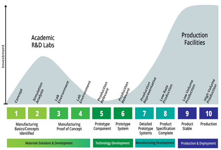
Currently, no two MIIs have the same structure or share the same business model. For one thing, they all focus on making investments in different fields where the technologies currently exist at different technology and manufacturing readiness levels (TRLs/MRLs). Nevertheless, they all share some commonalities. Because of the requirement to create and/or grow ecosystems, they all include strong education and workforce development goals and funding. They also seek to help bridge the manufacturing “valley-of-death” between MRLs 4–7, as depicted in Figure 4. Today, the MII with the most relevance for researchers in photonics is AIM Photonics (see Refs. [9] and [10]) so we will discuss this investment in terms of what it means for researchers in the field next. However, since there is always the possibility that a new MII will be created in another photonic-based area, my goal is primarily to use AIM Photonics to highlight this new concept/trend rather than for marketing purposes.
3. A New Mindset?
“Wait… I don’t have to make that all by myself anymore.?!”
Many groups/companies (be they academic, corporate, or government) have become adept at using e-beam and other specialty fabrication tools. Others have sought external support with electronic circuit design, packaging, etc. Today, there are a range of options that extend beyond doing everything yourself in your own group/company.
As a result, one of the biggest challenges may be for a group/company to decide on where their core expertise lies. This must also be reconciled with what commercial opportunities exist (for a company) and/or where the best funding options lie. Only with a strong understanding of these two things can the decision on what makes sense to do “in house” and when to leverage external partners be optimally made. This decision is frequently a pragmatic one that is based not only on the goals and objectives of the group/company but also on the expertise that exists within the group/company. While you are only as good as your people, it is also not wise to do everything yourself, even if you can. For example, who in photonics is out there making their own 1/4-20 screws because they have an employee who is skilled with a lathe? If there is a company doing this today, I would be curious to know how that’s working out for you.
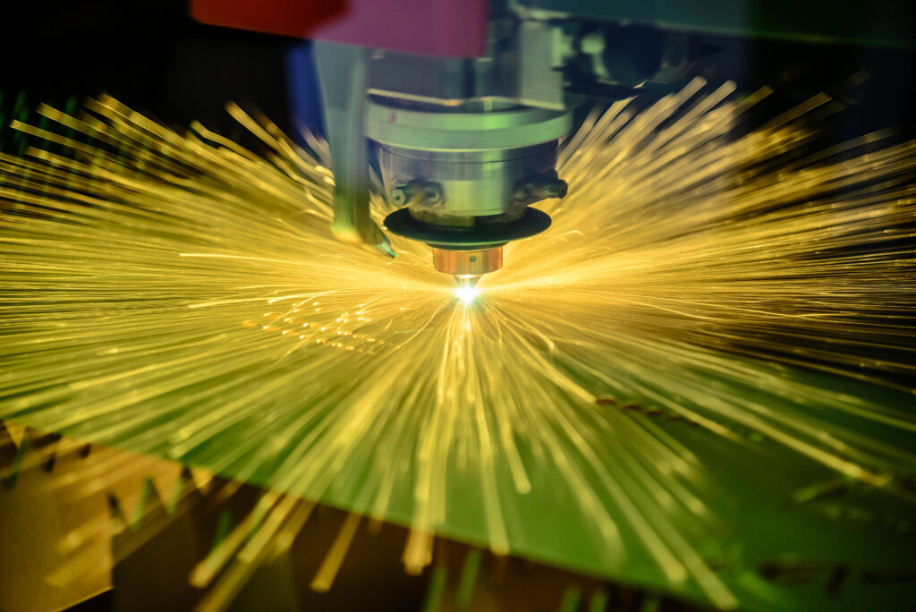
While it is unclear to me what future hardware companies will look like in fields that require substantial investments and/or advanced cleanroom facilities, it does make sense to look around at what capabilities exist elsewhere. For example, AIM Photonics was established (in 2015) because there were no multi-project wafer (MPW) offerings [see Note 2] for active integrated photonic circuits in the US. This changed when AIM rolled out its MPW offerings in 2016 (internally) and then in 2017 (to all). However, things have continued to evolve in the US since then and today researchers working in the field of integrated silicon photonics can also submit integrated photonic circuit designs to Tower Semiconductor [11] and Global Foundries [12]. There are also likely to be other options available to those in the field in the near future due to the CHIPS Act [13] and its associated funding. One area where there will likely be large investments made relates to the development of next-generation microelectronic packaging solutions. To what extent the photonics community will be able to take advantage of these is unknown but, since ~ 80% of the cost of photonics systems relates to their packaging, there are many reasons for companies to try to figure out if they will be able to take advantage of such investments should they materialize. Currently, AIM Photonics’ Test, Assembly, and Packaging (TAP) facility [14] represents a unique resource but one that is primarily focused on the packaging of integrated photonic circuits and, as such, is focused on supporting a specific community.
Still, having multiple options available forces one to make decisions regarding with whom to work. The effort of “qualifying a vendor” can be costly and time consuming and may shape how one’s group/company evolves. Fortunately, for those working in integrated photonics, I think these decisions are still relatively straightforward. For those with very high volume applications (> 10,000 wafers/year) Global Foundries represents the best choice. For situations where the volume is lower, some customization work is required, and 200 mm tools can be used, Tower Semiconductor would be a great choice. Finally, for those who want/require SoTA tools, only require low volumes (<100s of wafers/year), and/or require a good degree of flexibility, I would recommend AIM Photonics as the best option. Of course, for those who are still focused on research or developing a single type of device (laser, modulator, detector, etc.) and not concerned about making it available to others via a MPW platform, a university cleanroom may still present the best option. Finally, specialized low-volume work may be able to take advantage of some unique capabilities at Sandia National Laboratories or MIT Lincoln Laboratory.
5. Recommendations
I believe that advances in hardware underpin all true system advances. Because software development can improve the accessibility, ease of use, and value of many systems, and because it is less expensive than hardware development, software-centric companies have dominated Silicon Valley for more than a decade. Nevertheless, I think people will always desire better hardware and I view it as a noble challenge to advance the state of the art with respect to hardware innovation and through the creation of novel systems.
In finishing up this column, I would like to take the opportunity to throw some ideas out there for everyone working with hardware to consider:
For those currently in industry: I recommend you network at conferences, work with others as it makes sense, and good luck. I fear you may be undervalued in today’s world which has grown accustomed to expecting overnight successes and getting hardware (e.g. cell phones) for “free”. For those currently in academia: Yes, I know you love your job but, as I was told by the chairman of an Electrical Engineering department when I was looking at colleges as a high-school student: “the job of a good engineer is to create jobs.” This is a comment I have always remembered. If you are really good at your job, put yourself to the test and start a
company on the side. If it is going well, consider quitting your academic job, hiring your old students and others, and advancing the state-of-the-art, not through journal papers but by transforming society with your ideas via new products.
Many of your colleagues, whom I respect the most, have done just this. To be sure, it is scary and stressful, but I think they have found it to be rewarding and no one has yet to tell me they regretted it. Regardless of your field of expertise, consider recommending that your students look at a multitude of career options because we need good talent, not only in academia but also in industry and even in government.
For those still in graduate school: I recommend you envision your life 5, 10, and 15 years in the future. What makes you happy? Are you really attracted to one geographic area? Do you love a particular sport and want to live somewhere where you can do that more than anything else? What would you be willing to do for less than you may deserve, and would you make that trade? These are very tough questions for anyone to answer and it seems best to put them off until some point in the future. However, your life will unfold while you are still busy making other plans, so I recommend you talk to people at conferences across all job sectors and ask them not only “what they do” but “what they really spend their time on in any given week”. I would also encourage you to mentally prepare yourself to not spend your entire career still doing your thesis.
For everyone regardless of who you are or where you live: I also strongly recommend you consider your quality of life: what that looks like to you, what you value, and what you want. Is having an important-sounding job title important to you? Do you want to have a team of people working under you? Are you only motivated by salary? Do you want to just sit in a corner and do great research? Do you want to own a house? How much (job) uncertainty can you handle before becoming overly stressed out?
As a graduate student I was offered a job in an affluent area of California (Palo Alto). However, I was told by the senior manager of the organization that I probably would not be able to afford a house. I instantly realized that I would have a better quality of life if I took a job as a sanitation worker in upstate, NY. While that is not the path I chose, I think it highlights a useful exercise for everyone to go through when looking for employment.
I have long held the belief that fundamental research is best done in a monopoly or at least a company that has ample revenue to reinvest in itself without asking “what’s in it for me” or even worse “what’s in it for me this quarter.” Given the situation detailed above (where monopoly or monopoly-like companies are not running hardware-focused research labs), it is fair to ask the question as to where research can be best performed today? My conclusion on this matter, following the telecom bubble burst, is that academia and government laboratories, where the funding is not linked to commercial products but comes from a steady stream of guaranteed funding (from tuition or taxes), are one’s best bet.
For those seeking a career in applied research, opportunities in small companies are likely the best bet but there is a tradeoff to be made with job security and so such jobs may be best explored early in one’s career before the realities and responsibilities of life (e.g., having children) take over.
Advanced research is best done by companies that have existing product lines. This research, and anything that is more connected with a product, starts to look like what was noted earlier in this article as “reoccurring.” Such activities are typically tied to existing product lines. As a result, anyone seeking opportunities in this space, should familiarize themselves with the existing product lines of a given company prior to seeking employment.
6. Acknowledgements
The U.S. Government is authorized to reproduce and distribute reprints of this article (AFRL-2023-3486) for Governmental purposes, notwithstanding any copyright notation thereon. The views and conclusions contained herein are those of the author and should not be interpreted as necessarily representing the official policies or endorsements, either expressed or implied, of the United States Air Force, the Air Force Research Laboratory or the U.S. Government.
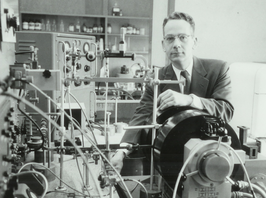
The author wishes to thank Robert Wilson for not only providing a higher-resolution image of Fig. 2, but also for providing additional information on its history.
7. References
[1] J. Gertner, The Idea Factory: Bell Labs and the Great Age of American Innovation (The Penguin Press, New York, 2012).
[2] V. Govindarajan and C. Trimble, Beyond the Idea: Hot to Execute Innovation in Any Organization (St. Martin’s Press, New York, 2013).
[3] https://en.wikipedia.org/wiki/Telecoms_crash
[4] M. Beranek, “The Role of Small Business Innovation Research in Defense Photonics,” IEEE Photonics Society News (July 2022).
[5] https://stockanalysis.com/stocks/kodk/employees/
[6] https://sites.nationalacademies.org/PGA/osaff/PGA_166302
[7] https://www.americamakes.us/
[8] https://www.manufacturingusa.com/institutes
[9] https://www.aimphotonics.com/
[10] N. D. Heidel, N. G. Usechak, C. Dohrman, and J. A. Conway, “A Review of Electronic-Photonic Heterogeneous Integration at DARPA,” J. Sel. Top. Quantum Electron. 22, 8300209 (2016).
[11] https://towersemi.com/technology/rf-and-hpa/silicon-photonics-rf/
[12] https://gf.com/manufacturing-services/multi-project-wafer-program/ [see the 45SPCLO offering]
[13] https://www.congress.gov/bill/117th-congress/house-bill/4346
[14] https://www.aimphotonics.com/tap
[Note 1] Historically, this is where venture capital (VC) funding used to help companies grow, but the track record of many photonics start-ups led VC firms to explore other sectors where the return-on-investment appeared to be better and safer. VC funding is also double-edged as it means corporate leaders must relinquish some degree of control and timelines are frequently greatly compressed.
[Note 2] For those not familiar with MPW offerings, it simply refers to collating the designs from many users and fabricating them on a single semiconductor wafer. In doing so, the overall fabrication costs are split by the riders with a small overall cost increase due to the additional work associated with design aggregation, dicing and shipping following fabrication.
A Bit About the Author:
Dr. Usechak received B.S. degrees with high honors in both electrical engineering and engineering physics from Lehigh University, Bethlehem, PA, in 2000. In 2003, he received an M.S. degree and in 2006 a Ph.D., both in optical engineering from the Institute of Optics, University of Rochester, Rochester NY where his dissertation focused on experimental work, numerical modeling, and the theory of FM mode-locked fiber lasers.
He worked at Trumpf Photonics in Cranbury, NJ as a Senior Engineer, for a year following graduation, characterizing high-power semiconductor laser arrays, automating experiments, and modeling the thermal effects of solder interfaces using transient temperature-extraction experiments to ground those models. After Trumpf he joined the Air Force Research Laboratory at Wright–Patterson Air Force Base where he is currently employed as a Principal Electronics Engineer. In addition to his research activities at AFRL, where he runs the Ultrafast Photonic Devices and Research Laboratory, Dr. Usechak also serves as the Program Manager for AIM Photonics, runs a number of AFRL contracts, and supports DARPA on a number of programs.
At Lehigh, he was a Presidential Scholar during the academic year 1999-2000. At the University of Rochester, he conducted his experimental work in the Laboratory for Laser Energetics where he was a Frank J. Horton Fellow. His research interests include integrated photonic devices and systems, nonlinear optics, fiber lasers, semiconductor lasers, ultrafast optics, high-speed test and measurement, high-power semiconductor lasers, mode-locked lasers, parametric processes, optical clock generation, novel gain media, diverse waveform generation, partial differential equations, delay differential equations, and numerical modeling.
Dr. Usechak is a member of the OSA, Tau Beta Pi, Sigma Xi, and a Senior member of the IEEE.
About the Column:
This is a regular column that explores the business aspects of technology-oriented companies, and in particular, the demanding business aspects of photonics startups. The column touches on topics such as financing, business plans, product development methodologies, program management, hiring and retention, sales methodologies, and risk management. We include all the pains and successes of living the photonics startup life.
This column is written sometimes by Daniel Renner and sometimes by invited participants so that we can share multiple points of view coming from the full spectrum of individuals who have something to say on this topic. At the same time, this is a conversation with you, the reader. We welcome questions, other opinions, and suggestions for specific topics to be addressed in the future. If you have any questions or comments, please send us a message at PhotonicsNewsroom@ieee.org.
The expectation is that this column will turn into a useful source of business-related information for those who intend to start, join, improve the operation, fund, acquire, or sell a photonic startup. A fascinating area for those who are lucky to enjoy it as a way of life.