Article © Copyright 2024 IEEE – The Institute. This article was written by Julianne Pepitone, a contributing editor covering consumer tech, cybersecurity, and business.
GE, IBM, and MIT’s Lincoln Lab announced the advance days apart
The semiconductor laser, invented more than 60 years ago, is the foundation of many of today’s technologies including barcode scanners, fiber-optic communications, medical imaging, and remote controls. The tiny, versatile device is now an IEEE Milestone.
The possibilities of laser technology had set the scientific world alight in 1960, when the laser, long described in theory, was first demonstrated. Three U.S. research centers unknowingly began racing each other to create the first semiconductor version of the technology. The three—General Electric, IBM’s Thomas J. Watson Research Center, and the MIT Lincoln Laboratory—independently reported the first demonstrations of a semiconductor laser, all within a matter of days in 1962.
The semiconductor laser was dedicated as an IEEE Milestone at three ceremonies, with a plaque marking the achievement installed at each facility. The Lincoln Lab event is available to watch on demand.
Invention of the laser spurs a three-way race
The core concept of the laser dates back to 1917, when Albert Einstein theorized about “stimulated emission.” Scientists already knew electrons could absorb and emit light spontaneously, but Einstein posited that electrons could be manipulated to emit at a particular wavelength. It took decades for engineers to turn his theory into reality.
In the late 1940s, physicists were working to improve the design of a vacuum tube used by the U.S. military in World War II to detect enemy planes by amplifying their signals. Charles Townes, a researcher at Bell Labs in Murray Hill, N.J., was one of them. He proposed creating a more powerful amplifier that passed a beam of electromagnetic waves through a cavity containing gas molecules. The beam would stimulate the atoms in the gas to release their energy exactly in step with the beam’s waves, creating energy that allowed it to exit the cavity as a much more powerful beam.
In 1954 Townes, then a physics professor at Columbia, created the device, which he called a “maser” (short for microwave amplification by stimulated emission of radiation). It would prove an important precursor to the laser.
Many theorists had told Townes his device couldn’t possibly work, according to an article published by the American Physical Society. Once it did work, the article says, other researchers quickly replicated it and began inventing variations.
Townes and other engineers figured that by harnessing higher-frequency energy, they could create an optical version of the maser that would generate beams of light. Such a device potentially could generate more powerful beams than were possible with microwaves, but it also could create beams of varied wavelengths, from the infrared to the visible. In 1958 Townes published a theoretical outline of the “laser.”
“It’s amazing what these … three organizations in the Northeast of the United States did 62 years ago to provide all this capability for us now and into the future.”
Several teams worked to fabricate such a device, and in May 1960 Theodore Maiman, a researcher at Hughes Research Lab, in Malibu, Calif., built the first working laser. Maiman’s paper, published in Nature three months later, described the invention as a high-power lamp that flashed light onto a ruby rod placed between two mirrorlike silver-coated surfaces. The optical cavity created by the surfaces oscillated the light produced by the ruby’s fluorescence, achieving Einstein’s stimulated emission.
The basic laser was now a reality. Engineers quickly began creating variations.
Many perhaps were most excited by the potential for a semiconductor laser. Semiconducting material can be manipulated to conduct electricity under the right conditions. By its nature, a laser made from semiconducting material could pack all the required elements of a laser—a source of light generation and amplification, lenses, and mirrors—into a micrometer-scale device.
“These desirable attributes attracted the imagination of scientists and engineers” across disciplines, according to the Engineering and Technology History Wiki.
A pair of researchers discovered in 1962 that an existing material was a great laser semiconductor: gallium arsenide.
Gallium-arsenide was ideal for a semiconductor laser
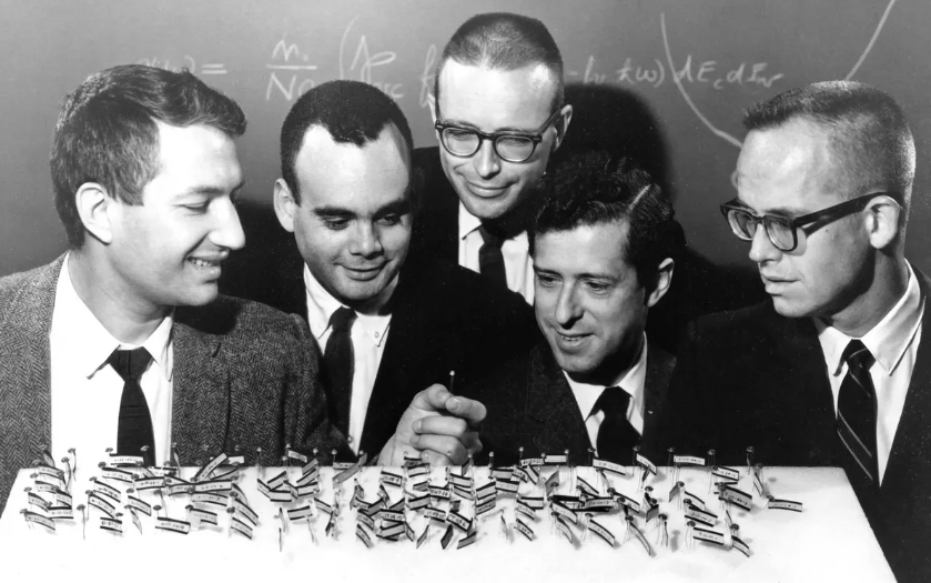
On 9 July 1962, MIT Lincoln Laboratory researchers Robert Keyes and Theodore Quist told the audience at the Solid State Device Research Conference that they were developing an experimental semiconductor laser, IEEE Fellow Paul W. Juodawlkis said during his speech at the IEEE Milestone dedication ceremony at MIT. Juodawlkis is director of the MIT Lincoln Laboratory’s quantum information and integrated nanosystems group.
The laser wasn’t yet emitting a coherent beam, but the work was advancing quickly, Keyes said. And then Keyes and Quist shocked the audience: They said they could prove that nearly 100 percent of the electrical energy injected into a gallium-arsenide semiconductor could be converted into light.
No one had made such a claim before. The audience was incredulous—and vocally so.
“When Bob [Keyes] was done with his talk, one of the audience members stood up and said, ‘Uh, that violates the second law of thermodynamics,’” Juodawlkis said.
The audience erupted into laughter. But physicist Robert N. Hall—a semiconductor expert working at GE’s research laboratory in Schenectady, N.Y.—silenced them.
“Bob Hall stood up and explained why it didn’t violate the second law,” Juodawlkis said. “It created a real buzz.”
Several teams raced to develop a working semiconductor laser. The margin of victory ultimately came down to a few days.
A ‘striking coincidence’
 A semiconductor laser is made with a tiny semiconductor crystal that is suspended inside a glass container filled with liquid nitrogen, which helps keep the device cool. General Electric Research and Development Center/AIP Emilio Segrè Visual Archives
Hall returned to GE, inspired by Keyes and Quist’s speech, certain that he could lead a team to build an efficient, effective gallium arsenide laser.
He had already spent years working with semiconductors and invented what is known as a “p-i-n” diode rectifier. Using a crystal made of purified germanium, a semiconducting material, the rectifier could convert AC to DC—a crucial development for solid-state semiconductors used in electrical transmission.
That experience helped accelerate the development of semiconductor lasers. Hall and his team used a similar setup to the “p-i-n” rectifier. They built a diode laser that generated coherent light from a gallium arsenide crystal one-third of one millimeter in size, sandwiched into a cavity between two mirrors so the light bounced back and forth repeatedly. The news of the invention came out in the November 1, 1962, Physical Review Letters.
As Hall and his team worked, so did researchers at the Watson Research Center, in Yorktown Heights, N.Y. In February 1962 Marshall I. Nathan, an IBM researcher who previously worked with gallium arsenide, received a mandate from his department director, according to ETHW: Create the first gallium arsenide laser.
Nathan led a team of researchers including William P. Dumke, Gerald Burns, Frederick H. Dill, and Gordon Lasher, to develop the laser. They completed the task in October and hand-delivered a paper outlining their work to Applied Physics Letters, which published it on 1 November 1962.
Over at MIT’s Lincoln Laboratory, Quist, Keyes, and their colleague Robert Rediker published their findings inApplied Physics Letters on 1 December1962.
It had all happened so quickly that a New York Times article marveled about the “striking coincidence,” noting that IBM officials didn’t know about GE’s success until GE sent invitations to a news conference. An MIT spokesperson told the Times that GE had achieved success “a couple days or a week” before its own team.
Both IBM and GE had applied for U.S. patents in October, and both were ultimately awarded.
All three facilities now have been honored by IEEE for their work.
“Perhaps nowhere else has the semiconductor laser had greater impact than in communications,” according to an ETHW entry, “where every second, a semiconductor laser quietly encodes the sum of human knowledge into light, enabling it to be shared almost instantaneously across oceans and space.”

Juodawlkis, speaking at the Lincoln Lab ceremony, noted that semiconductor lasers are used “every time you make a cellphone call” or “Google silly cat videos.”
“If we look in the broader world,” he said, “semiconductor lasers are really one of the founding pedestals of the information age.”
He concluded his speech with a quote summing up a 1963 Time magazine article: “If the world is ever afflicted with a choice between thousands of different TV programs, a few diodes with their feeble beams of infrared light might carry them all at once.”
That was a “prescient foreshadowing of what semiconductor lasers have enabled,” Juodawlkis said. “It’s amazing what these … three organizations in the Northeast of the United States did 62 years ago to provide all this capability for us now and into the future.”
Plaques recognizing the technology are now displayed at GE, the Watson Research Center, and the Lincoln Laboratory. They read:
In the autumn of 1962, General Electric’s Schenectady and Syracuse facilities, IBM Thomas J. Watson Research Center, and MIT Lincoln Laboratory each independently reported the first demonstrations of the semiconductor laser. Smaller than a grain of rice, powered using direct current injection, and available at wavelengths spanning the ultraviolet to the infrared, the semiconductor laser became ubiquitous in modern communications, data storage, and precision measurement systems.
The IEEE Boston, New York, and Schenectady sections sponsored the nomination, along with the IEEE Photonics Society. Administered by the IEEE History Center and supported by donors, the Milestone program recognizes outstanding technical developments around the world.
Spotlight photo caption: MIT’s Lincoln Laboratory’s [from left] Robert Keyes, Theodore M. Quist, and Robert Rediker testing their laser on a TV set. MIT Lincoln Laboratory


