IEEE Journal of Selected Topics in Quantum Electronics
DOI: 10.1109/JSTQE.2022.3222686
Are you feeling nostalgic for homogeneous integration of chips – one flat board where you can use your fingers to stuff in all the circuitry you need? Best to head to the Lego store or Russia. The rest of the world is moving fast to heterogeneous integration – where the boards are 3D, the chips are a mix of electronic and photonic functions, and every specification is in nanometers. It just as challenging as it sounds, but much more fun.
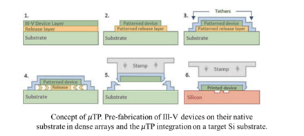
About 550 miles from Lego headquarters, in Belgium, a group of researchers have developed a new integration approach, micro-transfer printing (μTP), that combines the advantages of die-to-wafer bonding integration (high throughput integration) with those of flip-chip integration (pre-fabrication and pre-testing of the nonnative components, high alignment accuracy integration, no disruption of silicon photonics (SiPh) process flow). As you’ll recall, the salient process is flip-chip integration is that you put down an array of solder paste that looks just like the bumps on a Lego brick. Heat the assembly and the bumps form perfect little solder balls that conduct electric signals, thanks to the magic of surface tension. Yet grey solder is not the connection material for transmitting light. Instead, waveguides (aka wires for light) connecting photonic chips are either fabricated at the same time as the rest of the functional devices, or they’re made later when the photonic chips are on a silicon platform.
Printed electronic traces and conductive adhesives are used for flexible, commercial electronics today. Printing glass waveguides with a stencil or a 3D printer isn’t what this paper is describing. Instead, the researchers are describing a process more like embossing leather with decals or old-fashioned printing which was more like pressing a stamp down on paper. Remember silly puddy? It is 65% polydimethylsiloxane (PDMS). The stamp researchers are using is 100% PDMS and transparent.
So, imagine your Lego bricks are on the floor – various heights and shapes. To keep your glorious pattern, but move them all at once, you can stretch out silly puddy and press it into the Legos. Then you move the puddy, with the Legos attached over to a board. Press down. Gently peel off the PDMS. Voila! You have transferred Legos in a massively parallel way. The published design provides an impressive 1 μm lateral alignment tolerance. But why transfer at all?
The answer is that it is easier and cheaper to make “III-V devices” on a native substrate. Light-emitting devices need direct band gap materials like InP or GaAs. (These are III-V materials because they pair elements from groups three and five of the periodic table.) The Belgian researchers use III-V materials for their waveguides too. Ultimately though, these micron-sized parts must go onto a silicon substrate, because….economics.
The transfer technology is very versatile. Other demonstrations of μTP are underway, specifically: InAs/GaAs quantum dot lasers, Ce:YIG magneto-optic materials for optical isolators, periodically poled LiNbO 3 for nonlinear optics, BiCMOS electronics. Scaling up the technology to 200 mm and 300 mm wafers is underway. Researchers are continuously improving device performance (e.g., laserwall plug efficiency) and studying yield and reliability.
However, there is still a way to go for this technology to be used as a manufacturing technology. It’s a lot of work. Worried that it might take forever?
Note that this 14-page paper was authored by an extraordinarily well-educated group of 25 men and one woman. Most of the authors are/were nominally working at the University of Ghent. (Sarah is now a Photonics Engineer with Brolis Sensor Technology, Ghent, a high-tech company that designs and manufactures next generation infrared laser sensor systems where we hope she’s found some girlfriends to publish with.) Research at the university is intimately connected to Interuniversity Microelectronics Centre (Imec), an international research & development organization, active in the fields of nanoelectronics and digital technologies, with headquarters in Belgium.
Imec employs around 4,000 researchers from more than 90 countries. It has numerous facilities dedicated to research and development around the world, including 12,000 square meters of cleanroom capacity for semiconductor processing. Silicon photonics is in good hands.
-Beth Kujan
21-June-23