

June 24, 2026
Micro-transfer printing can enable heterogenous integration of diverse material systems in silicon photonics
Silicon photonics, which transmits data using photons instead of electrons, has emerged as a promising approach for overcoming bandwidth and latency limitations of electronic interconnects, key bottlenecks for upcoming artificial intelligence infrastructure. The platform is already widely used for photonic integrated circuits (PICs), particularly in telecom and datacom applications.
While silicon photonics are highly compatible with standard complementary metal-oxide-semiconductor (CMOS) technology and enable scalable PIC fabrication, current CMOS fabrication infrastructure is highly specialized and optimized and cannot integrate non-standard materials. Conventional group-IV semiconductor materials cannot satisfy all requirements of advanced photonic systems. In contrast, materials such as III–V semiconductors and lithium niobate (LiNbO₃) can fulfil these requirements, highlighting the need for heterogeneous integration methods.
A new study published in Journal of Lightwave Technology on April 30, 2026, highlights micro-transfer printing (MTP) as a promising approach for realizing heterogenous integration in silicon photonics. “Among the various approaches being pursued for enabling wafer-scale heterogeneous integration, MTP is an emerging highly versatile technique that combines benefits of die-level assembly with wafer-scale processing,” explains Ir. Ye Chen.
The study highlights the limitations of existing heterogeneous integration techniques and application of MTP to address them. Notably, one of the main advantages of MTP is its broad material compatibility, which allows multiple material systems to be integrated within a single architecture. This enables individual chiplets to be independently optimized using the most suitable fabrication processes before integration, while maintaining compatibility with CMOS-based photonic platforms.
Recent demonstrations of the MTP process include integration of indium phosphide (InP) and gallium arsenide lasers with silicon nitride (Si3N4) waveguides, wafer-level integration of LiNbO₃-based modulators with Si3N4 photonic circuits, and heterogeneous electronic/photonic optical receiver platforms.
“The MTP technology is still in its early stages of commercial application; however, we believe that consistent advancements will soon lead to large-scale industrial manufacturing, paving the way for advanced silicon photonics,” concludes Ir. Chen.
Reference
Title of original paper Journal Micro-Transfer Printing on Silicon Photonics: Tutorial, Recent Progress and Outlook Journal of Lightwave Technology
DOI
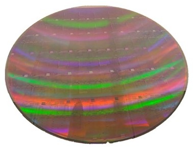
Image Caption: Micro-transfer printing enables highly flexible integration of two or more material systems in silicon photonics systems.
Press Release Source: IEEE Photonics Society
Media Contact First Name: Kristen
Media Contact Last Name: Amoroso Media Contact Email: k.amoroso@ieee.org
State of Origin: New Jersey, United States
Telephone: +1(732) 562-669